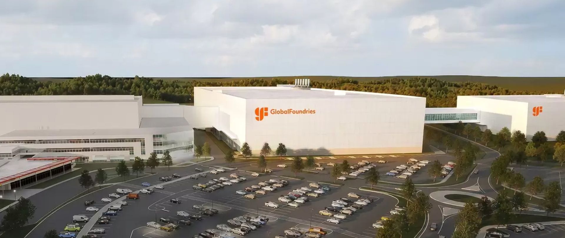
Eight years after GlobalFoundries abandoned the development of its 7nm FinFET technology, the company is preparing to return to 7nm-class performance, this time by going via a different route. Its FDX Fusion process, built on FD-SOI (fully depleted silicon-on-insulator) technology, promises 7nm-class performance using advanced planar transistors, with no EUV lithography necessary.
In an interview with Tom's Hardware Premium, GlobalFoundries' Sudipto Bose, vice president of the FD-SOI business unit, shared new details about its FDX Fusion technology, including its 8nm-class logic density, advanced planar transistors, manufacturing costs, and plans to begin commercial production in 2028. The company also explained how it intends to compete with conventional FinFET technologies and why it believes FD-SOI has a future beyond the 22nm-class generation. Some elements of this interview transcript have been edited for flow and clarity.
Sudipto Bose: I have been at GlobalFoundries (GF) for a little bit over six years, and I have been in the industry for 25+ years. I spent the rest of my career at Texas Instruments (TI), so it's really two jobs that I have done: TI and GF. Half and half engineering and business. I spent a lot of my business days in the automotive segment. This was what I was doing at GF when I joined, and now I have the FDX product line role.
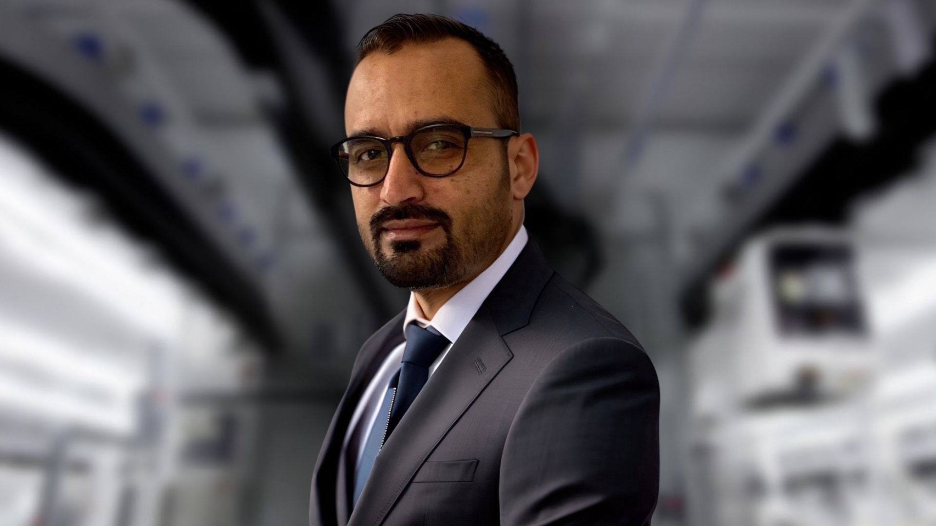
Sudipto Bose: A little bit on the history of FDX at GF. GF has been investing in FD-SOI for a long time. It started [these efforts] before I joined. So I would say almost eight years now. And a lot of the investment thesis that drove us towards FDX Fusion is based on the traction that we have in the market today, right? We have quite a few customers who are ramping up. And I say quite a few; this is like high double-digit customers in the nineties that are ramping up right now.
Applications for FDX Fusion
Anton Shilov: What specific types of chips and devices is FDX Fusion designed for? Which application will benefit most from its capabilities?
Sudipto Bose: FDX Fusion will try to enhance the applications in which we play today. What do I mean by that? If you look at our current customers, they are designing chips, everything to do with connectivity. When I say connectivity, think of Wi-Fi, Bluetooth, cellular, satcom, all of that. So that is one class of customers.
There's another class of customers who are designing processors at the edge, so these are MCUs (microcontroller units) with some level of inference sitting inside. Think of customers like Alif Semiconductors. So that is another class: MCUs at the edge.
Then in automotive, we have a disproportionate exposure to radar, and this is because of the eighty-one gigahertz performance that FDX brings to the table. So we will engage with them as they try to enhance their portfolio. We also have an automotive MCU, but radar is where you will see a lot of press releases that we have done.
Last but not least, we also have exposure in the data center segment. This also goes back to the fT/fmax, the high-performance RF that we have, which is a good candidate for designing TIAs and clock recovery circuits.
Anton Shilov: By applications inside data centers, what exactly do you mean? CPUs?
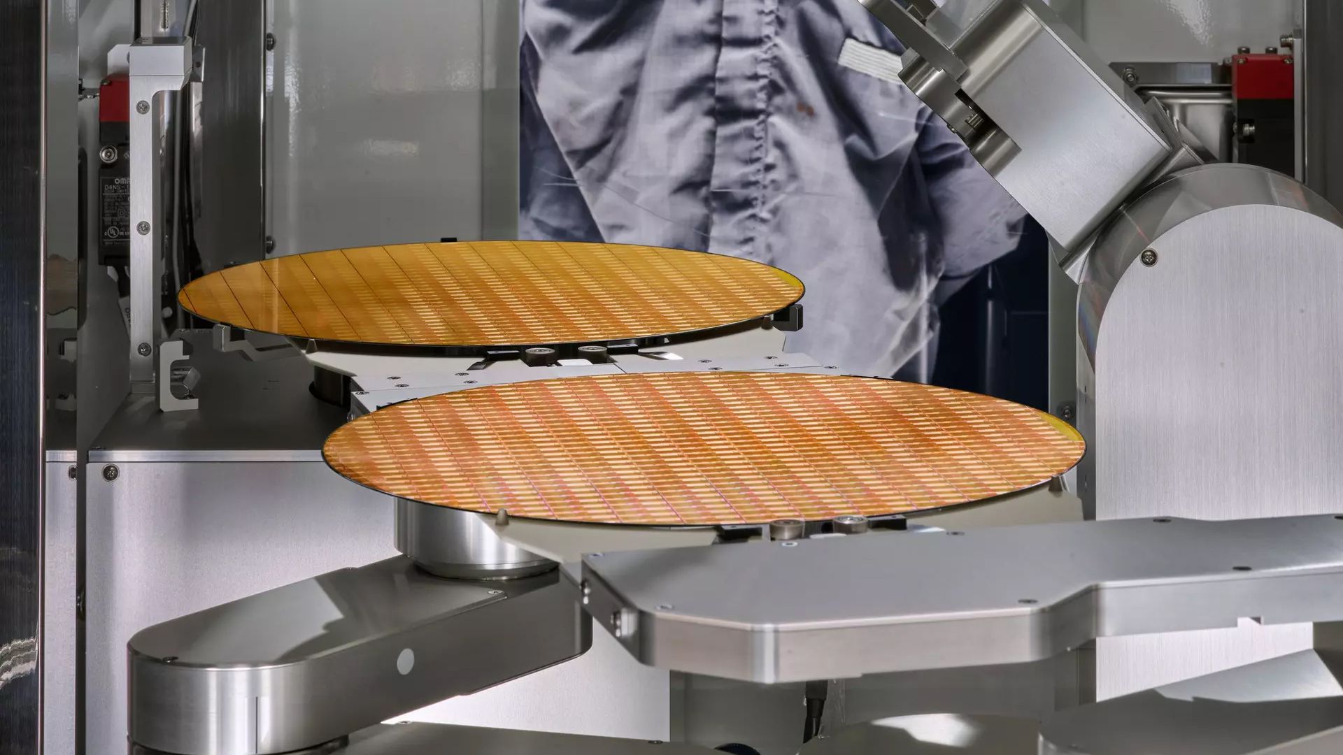
Sudipto Bose: Not CPUs. It is in the connectivity space. So, if you think about GF's focus, we are very focused on two things in data centers: power and connectivity. So in the connectivity space, we have silicon photonics, or turning electrons into photons. But then when you receive them, you have the optical diode, again, a GF silicon photonics technology. After that, you need circuits that will amplify those weak electrical signals and drive them to the compute chip. This circuit, which amplifies the weak electrical signals, is right now being done by GF silicon-germanium, but once FDX Fusion is there, we'll offer them both [as] options. And so, to be very specific to your answer, these are data/signal paths inside the data center that feed into CPUs.
7nm-class FD-SOI node
GlobalFoundries' FDX Fusion is a new manufacturing technology that promises 8nm-class logic density and 7nm-class power and performance without EUV lithography or FinFET transistors, which greatly reduces design costs and manufacturing costs at the cost of significantly lower transistor density compared to 7nm-class nodes.
Instead, the process relies on advanced planar fully depleted silicon-on-insulator (FD-SOI) transistors, strained silicon substrates, and aggressive optical patterning techniques to achieve transistor dimensions comparable to those of conventional 8nm-class FinFET nodes.
FDX Fusion also retains support for adaptive body biasing and combines high-density digital logic with RF, analog, and embedded memory capabilities. The technology will be manufactured using deep ultraviolet (DUV) lithography, although its tighter gate and metal pitches will likely require extensive multipatterning for the most critical layers.
Anton Shilov: What are the key innovations of FDX Fusion compared to predecessors and other nodes that are currently used?
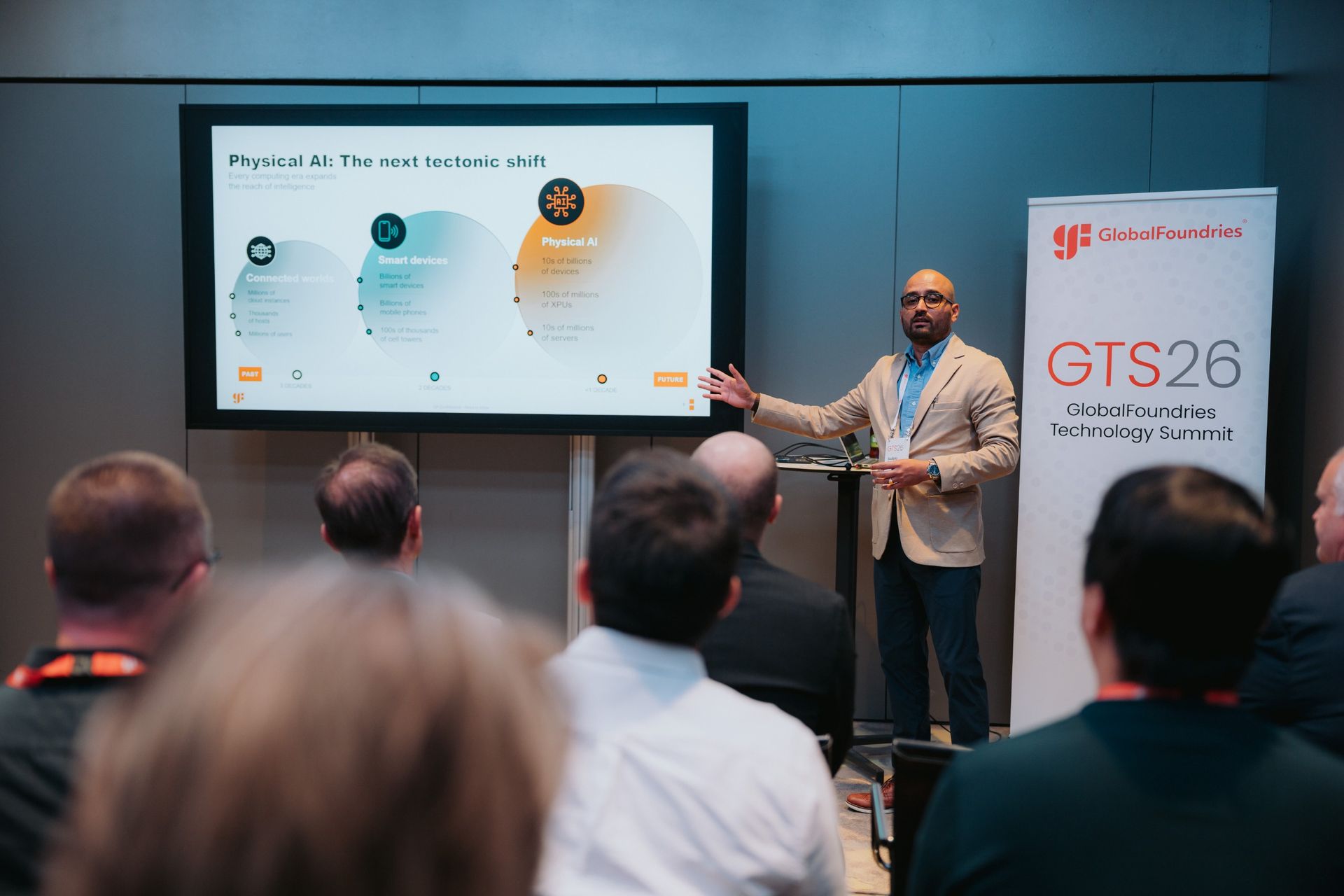
Sudipto Bose: The key things that we're improving from the current-generation FDX, the first one is fT/fmax, this is 500 GHz, or 0.5 THz fT/fmax. This helps the first segment that I talked about, which is connectivity. This helps automotive radar, and this definitely helps the data center segment as they try to improve data speeds. So this is not really competing with silicon germanium. Think of it as silicon germanium at the very high end, and FDX in the 100 – 200 Gb per lambda space. That is one. The second one is the inference at the edge. So we can call it physical AI, and we look at physical AI as sense, think, act, and connect. But the kind of feature set we are putting in starts with improving the digital gate density. This is 2.2 times more dense than the current generation FDX (22FDX and 22FDX+).
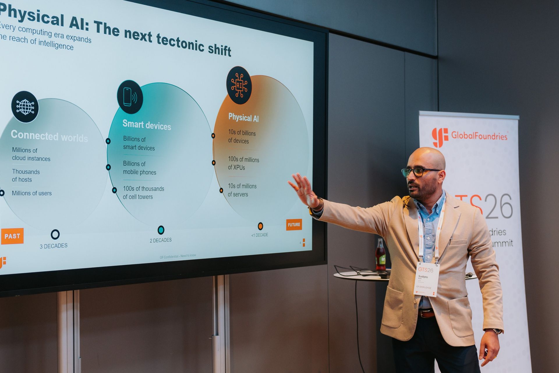
Sudipto Bose: We are putting in a lot of flavors of eNVM, a lot of flavors of SRAM, because in edge AI, and in fact for any AI, the real game is how much memory you can pack without increasing the cost. So we are adding a lot of flavors of those. The way we architected FDX Fusion is that we set a goal of how much performance we can deliver to our customer base without increasing their operating expenses.
If you look at classic 7nm, 6nm, they require EUV tools. The mask set is costly; the tool chain is costly. The FDX Fusion platform that we've built isn't going to use EUV tools. It is also based on planar technology. So there are two advantages to this. One is that we can support a much more competitive mask set price compared to 6nm. We can also offer [customers] a lot more flexibility in terms of cycle time and in how many places we manufacture, because FDX Fusion does not need EUV tools.
So, to summarize the answer? We are trying to improve RF and analog performance, digital gate density, and the classes of memory that we offer. What applications are we trying to target? It is connectivity, edge AI, high-frequency mmWave, automotive radar, and definitely applications inside data centers.
FDX Fusion vs FDX22 | FDX Fusion vs 12LP+ | FDX Fusion vs N7 | FDX Fusion vs 8LPP | Notes | |
Power | -40% | -20% | -5% | ? | At iso performance, ABB on for FDX |
Performance | 30% | 16% | 4% | ? | At iso power, ABB on for FDX |
Logic Density | ? | ? | ? | ? | - |
Transistor Desnsity (MTr/mm^2) | 2X vs 1X | 56 vs 30 - 40 | 56 vs 91.2 | 56 vs 61.2 | - |
Transistor Type | Planar vs Planar | Planar vs FinFET | Planar vs FinFET | Planar vs FinFET | - |
HVM | 2028 vs 2018 | 2028 vs 2017 | 2028 vs 2017 | 2028 vs 2018 | - |
Anton Shilov: You just mentioned transistor density. The press release says that it has more than twice the transistor density of the original 22FDX process, but you never actually published a transistor density number for this. Could you share any numbers?
Sudipto Bose: I will share a number with you. But I will also give you a little bit of context on how our customers look at our technology portfolio. If you look at the current generation, the one that we are manufacturing today, the one where I said we have 90+ customers ramping. Not designing, ramping. This basically comes from the flexibility of FD-SOI. You have the box, the depleted channel, and you can use body bias. So we have customers who are able to achieve 16nm-class power and performance with 22FDX. What do I mean by 16nm-class power and performance?
It essentially means that although our gate density is not as close to 16mm, when you look at the system-level requirements like CPU clock, but think of it as TOPS per watt, we are matching 16nm; in some cases, we are matching 12nm-class.
[...] If I were sitting in a time machine and went back seven years, instead of calling it 22FDX, we could have called it 16FDX, right? Or we could have called it 16nm-class FDX. So with that analogy, if you come to FDX Fusion, our gate density of FDX Fusion will be exactly the same as the industry's 8nm standard today.
It is 14 million gates per square millimeter; that is the density.
Note: Assuming he uses a two-input NAND gate as its reference, each gate contains four transistors, which translates to 56 MTr/mm², which is comparable to what Samsung's 8nm-class nodes use.
Sudipto Bose: Now, why do we call it 7nm-class? Or we actually thought of calling it 6nm-class, but then we said, let's wait for some silicon before we go too far ahead. It is because digital gate density is one aspect of a solution. It defines your physical size, the die size, and that is great. But then you need power and performance. And with the adaptive body bias (ABB) capability that FD-SOI has, and with the standard cell metallization innovations that we have brought in FDX Fusion, once a device is done and you again look at TOPS per watt, it should be equivalent, if not better, than what 7nm can achieve. That is our product target. So for a customer, the value it brings [customers] is: 'I do not have to use an EUV tool line. I do not have to use a mask set that costs many millions of dollars.'
I have something which costs a few millions of dollars, has great cycle time, but at the same time, I am getting TOPS per watt, which is similar to or better than 7nm. The die size might be bigger, but again, it should not be no bigger than what 8nm is today. And that is the messaging to the industry; that is why we say 7nm-class instead of saying, 'Hey, this is 7nm density.' We are trying to reflect what our customers have told us. That in the edge world, in the physical AI world, the size of the die is one aspect, but if the die does not meet the power requirement of the application, then the whole system will not function. So that is the push.
Anton Shilov: That is perhaps why you actually called the technology FDX Fusion instead of using some fancy number.
Sudipto Bose: Yes, because the moment we put a number [out], people put us in a box. And we want to give customers the optionality of, 'Listen, you want to design a transimpedance amplifier using the fT/fmax that we have? That's an analog circuit. No one cares about digital gate density. Go build it.'
'You want to build a simple MCU, which is just SRAM and IOs? We have 14 million gates per square millimeter. Go build it.' 'You want to build a mixed-signal design like a single-chip radar, Wi-Fi, a satcom digital beamformer? Here are the few other knobs that you can turn to get the best PPA or the best system performance that you need.'
That is why we chose the name Fusion; we are trying to imply [that] we give you many options. It is the combination of all the good things the world needs to design the physical AI dream that we have put in front of ourselves, like the whole stack concept of 'sense, think, act, and connect'. Let us see if it sticks. I think it is a bold move for us to go against the grain of the way the foundry industry typically names its platforms, but we feel pretty strong about it.
Anton Shilov: So, you shared the gate density number, but could you maybe also share things like contacted gate pitch, metal pitch as well?
Sudipto Bose: In time. The reason I mention that is there is a little bit of IP involved. We want to get the first silicon out, engage with a few customers before we publish the CPP and the M(etal) layers. […] We are pushing the limits of patterning and coloring as well as gate oxide engineering to get the best CPP and metal pitches, which will enable this level of density of gates. That is, I would say in terms of R&D dollars just at a very high level, 50% of R&D dollars is on the transistor itself because we are doing strained substrates. There are multiple techniques we are using to improve the PFET and NFET performance. The other 50% is all on CPP and metal pitches.
Anton Shilov: So, are those contacted gate pitches and metal pitches comparable to conventional 7nm class FinFET process technologies?
Sudipto Bose: Comparable to 8nm.
Anton Shilov: When we talk about 8nm, basically speaking, there is only one company that actually produces chips using an 8nm-class technology. That is Samsung Foundry. TSMC and Intel Foundry do not have 8nm-class technologies. So I suppose that we should compare it to Samsung's 8nm node, right?
Sudipto Bose: That's a fair guess.
Anton Shilov: When it comes to power consumption improvements versus 22FDX and 22FDX+, how much lower power can we get using the new FDX Fusion node?
Sudipto Bose: It depends on the application, but I understand your question. So if you just normalize with [iso performance and iso power], I am giving you an answer with adaptive body bias included. If you consider current-generation FDX as the base point, the goal of FDX Fusion is to get 30% higher performance and 40% lower power. Again, it is really application-driven [in] how low you can go. But if you take the standard core, our goal is to get at least a 20% improvement.
Anton Shilov: What types of chips do you expect to benefit most from the FDX Fusion technology? You mentioned connectivity, edge AI, high RF, automotive radar, and connectivity applications inside data centers. What about application-specific AI accelerators, because you mentioned edge inference?
Sudipto Bose: From the STAC — sense, think, act, and connect — framework point of view, let me give you an example. Think of a humanoid, or a car — major applications that need to see. It needs to see and then infer what the environment is like. So the class of chips that do this vision processing at the edge to infer the surroundings will definitely be supported with FDX Fusion. The class of chips that will hear, do voice recognition, and, from voice recognition, draw conclusions, we definitely want to support [them]. Now, at the data center right now, as I said, our play is connectivity. Just translating optical to electrical signals.
If a customer wants to use a chiplet, which has a lot of memory, think of analog in-memory compute along with an inference engine, by all means we will support [such applications]. We will work with customers to see how we can play in that compute ecosystem in the data center. But in terms of pure focus, the first 10 customers that we are engaged with are either at the edge, or they are in the connectivity piece inside the data center.
Note: For those of our readers who are not familiar with ABB, this is a technique that dynamically adjusts a transistor's threshold voltage by changing the voltage applied to the transistor body. Forward body bias reduces threshold voltage to improve performance, while reverse body bias increases it to reduce power leakage. This enables chips to optimize performance and power consumption according to workload requirements. ABB is one of the key advantages of the FD-SOI technology.
Anton Shilov: Since you mentioned this, does FDX Fusion retain the active body biasing capabilities of its predecessors?
Sudipto Bose: It is an inseparable part of the platform, yes. We will launch this platform in a way that customers can use it.
New tools required
Anton Shilov: You also mentioned makers of wafer fab equipment. Will FDX Fusion use existing manufacturing equipment at the Dresden facility, or will it require substantial investments in new lithography, deposition, etching, and metrology tools?
Sudipto Bose: It will require new tools. Substantial is a relative term. If you see the amount of money being invested in semiconductors, the term 'substantial' has changed. We are going to get new tools, which is why we combined the FDX Fusion announcement event with the topping off of the Sprint expansion project. That's why we had all the luminaries from the German and the European government. There will be tool investment; we will be buying tools from the vendors. How much of it is going to be litho versus etching? Time will tell, but for sure we need new tools compared to what we have today.
Anton Shilov: But will you essentially need to completely re-equip the Dresden facility to use FDX Fusion? What percentage of the tools you have can be reused for FDX Fusion?
Sudipto Bose: We can get back to you on that exact answer because I do want to give you a proper answer, rather than a high-level answer. But I will tell you where the targets are. With the front end, the transistor fabrication tool chain, my target is to reuse as much as we can.
Anton Shilov: You also mentioned that you plan to begin manufacturing FDX Fusion in 2028. But does this refer to risk production, initial customer production, or high volume manufacturing?
Sudipto Bose: Initial customer production.
Anton Shilov: When do you expect the technology to reach mature yields and meaningful production volumes?
Sudipto Bose: I will give you my target, and then the industry will define it because we are a part of a bigger ecosystem. 2030 is when we want to get to high-volume manufacturing with FDX Fusion. But again, it depends on the first applications and the first few customers.
Readiness
Anton Shilov: Speaking of customers, you probably already have customers who are committed to production, haven't you?
Sudipto Bose: We have customers who are committed to building a chip. Of course, we have to deliver to their specs before they go to production.
Anton Shilov: I suppose the customers that you mentioned in the press release like BMW, Bosch NXP, Siemens, and Tesla, they are all plan to build chips on this technology.
Sudipto Bose: […] They have been pushing us for the last few years to do something like this, and they have given us requirements. Now we are doing it, and we have to show them what we can [deliver]. So there is a lot of push that we have received from the industry, from these companies. When I say these companies, the supply chain that leads into these companies to deliver something which will work at the edge. So we are racing against time to show them something that will meet the specs.
Anton Shilov: GlobalFoundries plans to release the initial FDX Fusion PDK in mid-2027. But when do you expect complete digital, analog, and RF design flows to become available from the three major EDA vendors?
Sudipto Bose: Yeah. I wish I could tell you… Right now we are in discussion with all the major primes, so we are in the request for information/request for quotation (RFI/RFQ) phase, but we have started discussions with the major EDA vendors. It has been almost six to nine months now.
Anton Shilov: But you do expect all the leading EDA vendors to support FDX Fusion in eight to nine months?
Sudipto Bose: Of course. We are going to engage with the whole ecosystem that we have, and once [the PDK is out], we have to support a proper flow not just for chip design, but also IPs that are required and everything else around it.
Anton Shilov: So how extensive will the initial FDX Fusion IP ecosystem be? Will customers have access to silicon-proven standard cell libraries, SRAM compilers, embedded non-volatile memory, interface IPs, maybe analog and radio frequency building blocks before 2028?
Sudipto Bose: Yes. In the first two years, we are going to engage with pilot customers. Think of these as early adopters. We have early adopters listed, and we will design standard cell, I/Os, and SRAM [...] needed for everything, so we will have those. But then the complex IPs, like PCIe Gen 4/5 or LPDDR6 or a DisplayPort, will be dictated by the first few applications that will ramp. FDX Fusion for us is the beginning of a journey. We have been on the journey of 22FDX for almost eight years. I envision FDX Fusion to be more than that. Even on our current platforms, we keep enhancing our IP portfolio. So I expect us to be adding IPs to FDX Fusion over the next ten years.
ARC, MIPS, and Fusion FDX
Anton Shilov: GlobalFoundries also highlighted its ARC and MIPS processor IP portfolios and RISC-V expertise as part of the FDX Fusion offering. Do you plan to develop processor cores and AI accelerators specifically optimized for FDX Fusion? IPs specifically optimized for FDX Fusion? Or will you primarily port existing IP to the new process?
Sudipto Bose: MIPS is an internal customer and a partner, and we will engage with them, and they will launch a platform for physical AI that is fine-tuned, in a combination of what they have and what FDX Fusion has. ARC and MIPS are key pieces of the strategy. Having an internal customer like that just enhances our development cycle by 5X because now they can start developing fast turns of test chips and give us feedback. We did not have this capability in the past. Now we do. Once they are ready, they will start announcing stuff.
Anton Shilov: So essentially, you will both port the existing IPs to the new node, but also MIPS will likely develop something brand new specifically for FDX Fusion.
Sudipto Bose: Yes.
Costs
Anton Shilov: How will the manufacturing complexity and cost per transistor of FDX Fusion compare to 22FDX+, your 12nm FinFET technology, and conventional 8nm FinFET technology?
Sudipto Bose: This would be the most advanced planar transistor that the world has seen, the most advanced non-EUV-based manufacturing line that the world has seen. So, I would say significantly more complex than our current 22nm-class FD-SOI line. More complex than what we have on the 12nm FinFET line. We are working with every tool vendor that you can think of as part of this program, and we have given them the challenges. It goes back to your question about our contacted gate pitch and metal pitch. So, we have had multiple workshops with them over the last few quarters, and each one of them is proposing a tool recipe that they think will get this to a nice and solid yield.
Sudipto Bose: So, I guess the answer to your question is: firstly, it is definitely complex, and secondly, we are really using the entire ecosystem available to us to come up with tool configurations that will deliver this. All of this is going to happen in Dresden. We have to be competitive, so price is always dictated by the market. Our goal is to have a running cost that is significantly better than a 7nm or a 6nm class of design (due to planar transistors and due to lack of EUV masks). After that, we will work with our customers to figure out what makes sense. But you are right, the value that we want to bring in is, 'dear customers, you do not have the same operating expenses load, meaning the cost of tape-out is less than 6nm.'
And you can do multiple tape-outs because this class of devices is not something where you can design one part and use it for 15 applications. You really need 15 devices for 15 applications. So, we definitely enable that. Then, when it comes to manufacturing cost, it is a discussion with our customers. We have various business models, but the goal is to make sure it is a win-win. At the end of the day, the lower the cost we are, the more flexibility we can provide to our customers. The non-EUV path is one of the things that was dictated by our decision that we must keep this a cost-competitive platform.
Anton Shilov: So, cost-wise you want to be competitive, but it's likely comparable to 8nm.
Sudipto Bose: I will have a better feel once we are complete with what we call our M-cycles inside the fab. But I would say my internal target is that we have to be better than that.
The future of FDX
Anton Shilov: GlobalFoundries describes upcoming technology as its 1st Generation of FDX Fusion. Does this mean that you envision subsequent generations with high transistor density and performance? Maybe you can share some preliminary targets or timelines for the next node?
Sudipto Bose: We have listed quite a few innovation steps that we want to enable on this platform. The FDX Fusion definition is based on the ones we believe we are more confident that we will be able to deliver in the timeframe that we have said. We have kept a few things in the innovation lab, and they are pushing the boundaries of a few things like eNVM, EDA routing, chip folding, 2.5D integration, which, once they mature, will define what the next version of FDX Fusion will look like. I do not have a timeline for the next version of FDX Fusion, though.
As we proceed through the development phase, I would say early 2028 to mid-2028 is when I expect to have a better view of when the next version will be launched. And this is also based on feedback we will get from customers. Because what we have right now is our first silicon, which is running in the lab, which we will show to customers. They will give us a lot of feedback. I am sure we will get a few things right, and at the same time, we will get a few things not so right. And that feedback, along with a few of the innovation topics I mentioned, will dictate what the next generation is going to look like. Stay tuned!
Anton Shilov: One of the reasons why I aksed about next-generation nodes is partly because TSMC typically shares its process technology roadmaps with new nodes well before it releases early PDKs for these nodes. Given that FDX Fusion is now GF's most advanced logic process, with capabilities comparable to 8nm-class technologies (i.e., more advanced than 22FDX or bulk 12nm FinFET), how frequently does GlobalFoundries plan to introduce new process technologies, and how far in advance will it disclose its roadmap?
Sudipto Bose: I would say, we are doing advanced development across the board. If you look at the work we are doing on silicon photonics, on packaging, on power transistors like GaN, RF GaN, Power GaN, these are all pretty advanced. But yes, you are right: in what the world understands as a classic, let's say, high-density process, FDX Fusion is the most advanced. We typically announce or update the industry about our roadmap every year at the GlobalFoundries Technology Symposium. Like this year at GTS, we announced FDX Fusion. So, I would say stay tuned for the GTS sessions that we have, and typically every year we do it in September or October.
CEA-Leti involvement
Anton Shilov: CEA-Leti describes FDX Fusion as a single-digit FD-SOI node. How closely is this new technology related to CEA-Leti's own research in 10nm and 7nm with their SOI nodes?
Sudipto Bose: The platform that we have right now is the outside of the substrate engineering work that we are doing with Soitec and CEA-Leti; the rest of it is GF inherent IP at this point in time. So we are bringing in the knowledge that we have from current-generation FDX, the knowledge that we have from the work that we did in 7nm before we stopped it, the work that we have done on 12nm. So it is bringing in all the innovations across all the GF fabs to figure out what is the best that we can offer. Does it mean that we will not look at what CEA-Leti has in the future? I do not have an answer right now. But for now, FDX Fusion is a very GF innovation-driven effort.
Anton Shilov: So you did not use pre-competitive IP from CEA-Leti to develop FDX Fusion? Is it a completely internally developed node?
Sudipto Bose: Correct.
Anton Shilov: The press release mentions innovations in substrate engineering along with endorsements from CEA-Leti and Soitec. What exactly does that involve, and how does it improve transistor performance? What role do Soitec and CEA-Leti play in developing FDX's strained silicon substrates, and how close is this technology to mass production?
Sudipto Bose: GlobalFoundries is working with CEA-Leti and Soitec under the FAMES program to develop strained silicon substrates for FDX Fusion. The goal is to improve charge carrier mobility and, consequently, transistor performance. Since FD-SOI technology relies on specialized silicon-on-insulator wafers supplied by Soitec, the three organizations are developing ways to introduce strain into these substrates and make the technology suitable for high-volume manufacturing. The approach has already demonstrated its viability in the laboratory, and the partners are now refining the manufacturing process to prepare it for commercial production.
[Session ends]