Intel Foundry last week made available its Intel 14A process design kit (PDK) version 0.9, an important milestone in the development of this next-generation manufacturing technology. The company says that the production node is reaching performance and yield maturity expected at this stage of development, and the results are backed by silicon validation. Intel plans to release PDK 1.0 in the first quarter of 2027, which will validate the technology's readiness for high-volume manufacturing (HVM).

14A PDK v0.9 is here
A process design kit contains transistor models, design rules, and other information that enables chip designers to develop products for a particular manufacturing process using electronic design automation (EDA) tools. The accuracy and quality of the PDK are crucial for modelling how chips will perform once manufactured, and the release of PDK 0.9 is particularly important because it provides customers with a representation of Intel 14A based on actual silicon measurements rather than on theoretical models or simulations. At this stage, customers can proceed with product development with greater confidence that the technology will meet their requirements when it comes to performance and power consumption.
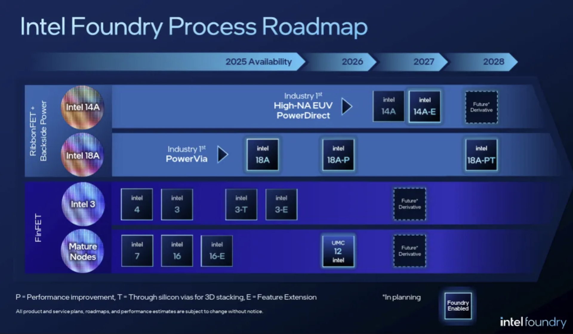
Intel says that PDK 0.9 lets customers develop designs intended to enter risk production around the time the process is certified, which — provided that PDK accurately reflects the characteristics of manufactured silicon — in many cases enables chip developers to greatly reduce the number of silicon revisions between initial tapeout and mass production. Of course, availability of PDK 0.9 does not indicate that Intel 14A is ready or even close to mass production, as the company expects to validate HVM readiness only with PDK 1.0, sometime in Q1 2027. Again, this does not mean that 14A will enter mass production in early 2027, as Intel itself expects to begin mass production using its 14A process technology in 2028, following risk production for its own products in the second half of 2027.
"From a customer perspective, the PDK 0.9 gives customers the confidence to design products on Intel 14A, as the technology is reaching the industry-standard performance and yield maturity expected at this stage of development, supported by silicon-backed validation," said Ben Sell, corporate vice president and general manager of front-end technology development at Intel Foundry.
Building on top of 18A
Intel 14A builds on top of architectural foundations introduced with Intel 18A but incorporates several substantial enhancements. These include 2nd Generation RibbonFET 2 gate-all-around (GAA) transistors, PowerDirect backside power delivery (which delivers power right to the transistor source/drain regions without using intermediate connections like TSVs used by PowerVia), and Turbo Cells (high-performance standard cells designed to accelerate timing-critical paths in CPUs and GPUs), which provide chip designers with additional ways to increase performance and optimize power efficiency. Since Intel has previously outlined advantages of these technologies, the latest announcement does not provide updates regarding transistor performance, power consumption, or transistor density figures for Intel 14A.
Beyond improvements to transistor, power delivery, and interconnect technologies, Intel is applying manufacturing experience gained during 12 months of Intel 18A production to accelerate maturation of 14A. Specifically, the company says it has increased investments in inline defect detection, modeling, and simulation to identify potential manufacturing problems earlier in the development cycle. These initiatives are intended to improve manufacturing yields, process variability, ultimately transistor performance, and reduce production cycle times. Intel also says it has introduced several strategic initiatives to accelerate technology development, although it does not quantify their impact.
New collaboration model
Another important change concerns Intel's relationships with equipment and materials suppliers. The company says it has revised its collaboration model to involve technology development teams and external suppliers earlier in the process development cycle. The goal of such close collaborations is to address manufacturing defects and improve equipment capabilities before they become obstacles for yield improvements after the technology enters mass production. Intel also conducts regular yield summit meetings with suppliers to accelerate progress on critical development objectives.
"This has required evolving our collaboration model with equipment and material suppliers, and earlier engagement from our [technology development] leaders with suppliers to drive improvements in defects and equipment capabilities," Sell said.

A bonus of such early collaboration is that equipment and materials suppliers may incorporate Intel's requirements into their standard products and development roadmaps. This could give Intel an advantage over competitors, which would have to either adapt their manufacturing processes to equipment optimized around Intel's requirements or work with suppliers to develop alternative solutions from scratch.
Historically, Intel frequently set the direction for semiconductor manufacturing technologies as other chipmakers subsequently adopted similar approaches. One notable exception was immersion DUV lithography, which Intel adopted after TSMC, which led the development of immersion DUV lithography. By engaging equipment and materials suppliers earlier, Intel could regain some of its historical influence over the development of industry-standard manufacturing solutions, though the importance of this should not be overestimated.
Expanding design ecosystem
Meanwhile, Intel continues to expand the design ecosystem for its 14A technology. Cadence and Intel have established a design-technology co-optimization (DTCO) collaboration focused on next-generation AI-driven design tools and intellectual property, whereas Keysight, Siemens, and Synopsys have announced design-tool certifications for the process. Intel is also working with other software developers and IP providers to validate design flows and reusable building blocks required by prospective foundry customers.
Intel says it is encouraged by customer feedback regarding the progress of 14A development. However, the company has not identified any customers that have committed to manufacturing products using the technology, disclosed customer tape-outs, or announced specific manufacturing agreements, which is normal for the foundry industry. For Intel Foundry, attracting external customers remains particularly important because development costs of modern leading-edge process technologies can only be recoupled when they are used to make hundreds of millions of chips, way more than Intel sells these days. Meanwhile, the commercial success of Intel Foundry with advanced manufacturing technologies depends not only on transistor performance and manufacturing yields, but also on its ability to deliver predictable development schedules.
Looking ahead, Intel intends to continue improving performance, yields, variability, and manufacturing cycle times of 14A, though for now the company does not disclose any actual goals. Intel also plans additional process enhancements and performance refinements for 14A-E and 14A-P nodes after the initial technology becomes available. However, exact schedules for these nodes are not known at the moment.
"Our next major milestone is the Intel 14A PDK 1.0, expected in the first quarter of 2027," said Ali Farhang, corporate vice president and general manager of Intel Foundry's design technology platform organization. "I am looking forward to sustaining this level of quality across future releases and continuing to earn our customers' trust by delivering on our commitments with a customer-first mindset."